IEEE Spectrum: Cash Comes in for Nanowire Display Startups
While much of the near-term innovation of future TVs will come from the processing horsepower behind the screen, farther out you can expect a big change in the pixels themselves: nanowire displays, or micro-LEDs. These displays would be made up of pixels made of miniaturized gallium-nitride LEDs, which are so efficient that displays would consume half or even one-third of the energy used by OLED or LCD displays while being considerably brighter than both.
Samsung, seemingly at great cost, assembled a huge microLED display for CES that it called “The Wall,” but the technology is likely to make its mark much sooner in small displays for augmented reality and smartwatches. Apple, for example, acquired micro-LED display startup LuxVue in 2014, which reportedly had raised $43-million to that point. MicroLED displays still haven’t appeared in the Apple Watch, though.
In the past four months, venture capital groups have poured cash into two microLED startups whose particular take on the technology could speed up its adoption. Both rely on growing nanometer-wide wires that each comprise an LED. In August, Glo, founded by Lund University nanowires expert Lars Samuelson and based in Sweden and Silicon Valley, got SEK241 million (US $15 million), with Google leading the investment. And in January Aledia, a spinoff of CEA in Grenoble, France, took in €30 million (US $37 million), adding Intel Capital to its investors.
“This is going to be a generational shift in technology,” says Aledia’s CEO, Georgio Anania. The main advantage of using gallium-nitride LEDs as pixels is efficiency. Today’s technologies, LCDs and OLED displays, are only around 5- to 7-percent efficient. But the efficiency of gallium-nitride LEDs for lighting is closer to 70 percent. Efficiency degrades as you make the LEDs tinier and tinier, Analia points out, but even a 15-percent-efficient display “would be a revolution.”
But gallium-nitride is expensive, costing multiples of silicon, so you have to limit how much of the material is used. Even for LEDs destined for lighting applications, the gallium nitride is grown as a thin layer atop a wafer of sapphire and in some cases silicon. Sapphire is used because its crystal lattice matches that of gallium nitride pretty well. That matchup means the gallium nitride grown atop it has few defects. In larger LEDs, the defects can sap power. But in the tiny ones needed for displays, it can kill the device entirely.
In an effort to make LEDs cheaper by using a more plentiful starting wafer that comes in larger sizes, LED makers have worked hard on ways to grow gallium nitride on silicon. Silicon isn’t a natural fit, so there are bound to be more defects. Part of Aledia’s allure is that those defects don’t matter much to its nanowire LEDs.
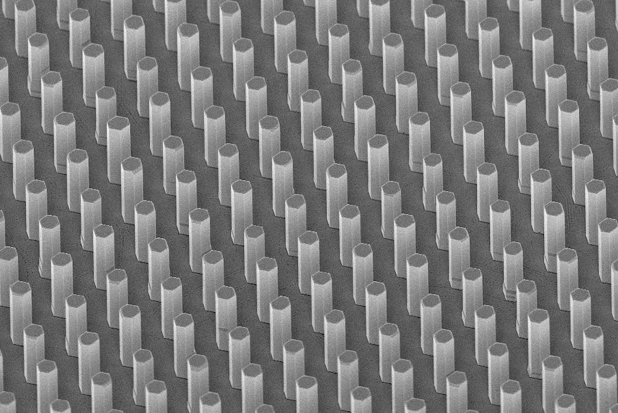
The company grows fields of gallium nitride nanowire LEDs on 200-millimeter silicon wafers. Each nanowire has an inner and outer core of gallium nitride sandwiching a series of what are called quantum wells—very thin layers of material that confine charges and have the effect of enhancing the recombination of electrons and holes to produce light. Doping the structure with specific types and concentrations of atoms makes LEDs that shine in either red, green, or blue.
In gallium nitride–on-silicon systems defects can occur because the two materials expand at different rates when heated. This stresses the gallium nitride, creating dislocations in its crystal structure. But nanowires have such a small footprint that the resulting stresses across one of them are pretty small. Even if a defect does occur, there are potentially hundreds of nanowires in each pixel, so one dud doesn’t make a difference.
Still, duds are a big problem for a display that’s supposed to be made up of thousands of individual LEDs. Such displays would be made by placing each tiny LED onto the screen substrate. If one LED doesn’t work, the whole screen is a waste. Samsung’s Wall demo is a 4K TV; meaning it had, at minimum, a preposterous 8.3 million perfectly operating, perfectly placed LEDs.
For large displays, Aledia’s advantage is that there will be no duds. But for small displays, such as smartwatches or the microdisplays that will enable future AR and VR systems—and someday even contact-lens systems—Aledia can take further advantage of its silicon base. It can build the whole display out of a single nanowire-studded silicon chip.
Such monolithic displays can have the silicon portion fully processed into the needed circuits to drive the pixels, and then the gallium nitride LEDs can be grown right on top, says Anania. The company’s first target is monolithic displays for smart watches and other small forms. It’s closest to producing such a display using only blue pixels, which would then be converted by phosphorescent chemicals to produce green and red.
But “Silicon Valley wanted native RGB,” he says. So the company is working on making pixels containing nanowires that have different chemical doping profiles to produce all three colors. “We’re still working through the tech challenges,” says Anania. “A display is a complicated subsystem.”
Read more on IEEE Spectrum here.


